SEMulator3D FinFET Process Model
sketchfab
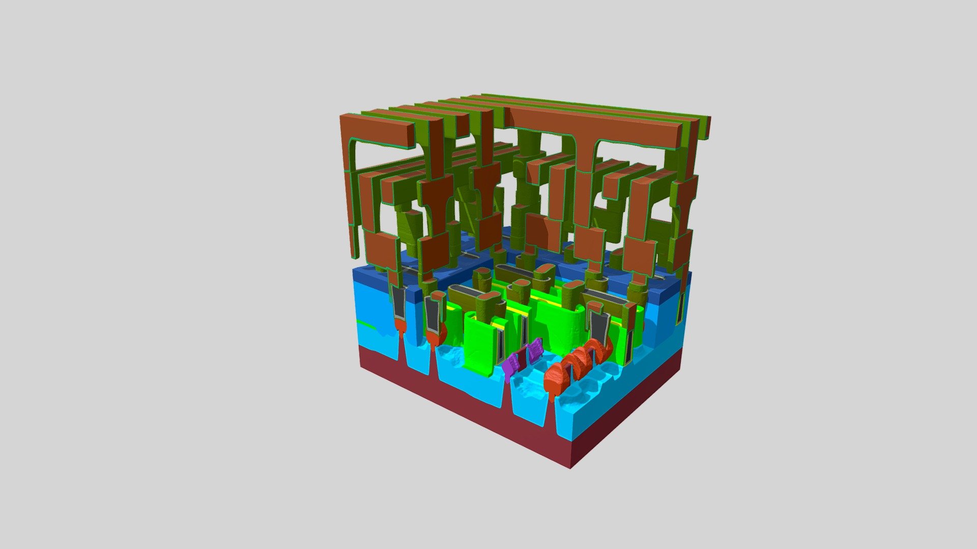
Using a state-of-the-art semiconductor process simulation developed by Coventor, this 3D model showcases a small segment of a FinFET device in stunning high resolution. The graphic displays a portion of the structure that measures approximately 600 nm on each edge - roughly equivalent to the wavelength of orange light. Each of the 17 distinct colors represents a different material used throughout the manufacturing process. The model is fully integrated, highly predictive and extremely accurate, displaying all processes from the initial wafer preparation through FEOL to the final back-end metal layers. It highlights the advanced virtual wafer fabrication capabilities of SEMulator3D, including MultiEtch, Visibility-Limited Deposition, Selective Epitaxy and other cutting-edge semiconductor fabrication processes. Credit: Peter Fried, ARC-3D and the NYU Department of Applied Physics
With this file you will be able to print SEMulator3D FinFET Process Model with your 3D printer. Click on the button and save the file on your computer to work, edit or customize your design. You can also find more 3D designs for printers on SEMulator3D FinFET Process Model.