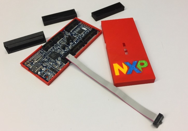
NXP LPC-Link2 Enclosure
thingiverse
A Custom-Made Enclosure for the NXP LPC-Link2 Debug Probe Board Takes Shape. The NXP LPC-Link2 debug probe board is a widely used tool among developers, and now it has a sturdy enclosure to match its versatility. The design of this enclosure does not require any screws, making it easy to assemble and disassemble as needed. A key feature of the enclosure is its handle, which provides a convenient place to store the SWD debug cable when it's not in use. This thoughtful touch adds to the overall functionality of the enclosure, allowing users to keep their workspace organized and clutter-free. For those interested in building their own custom enclosure, detailed instructions can be found on the MCU on Eclipse website. The link provided offers a step-by-step guide on how to create this enclosure using 3D printing technology.
With this file you will be able to print NXP LPC-Link2 Enclosure with your 3D printer. Click on the button and save the file on your computer to work, edit or customize your design. You can also find more 3D designs for printers on NXP LPC-Link2 Enclosure.
