Connected Cube
sketchfab
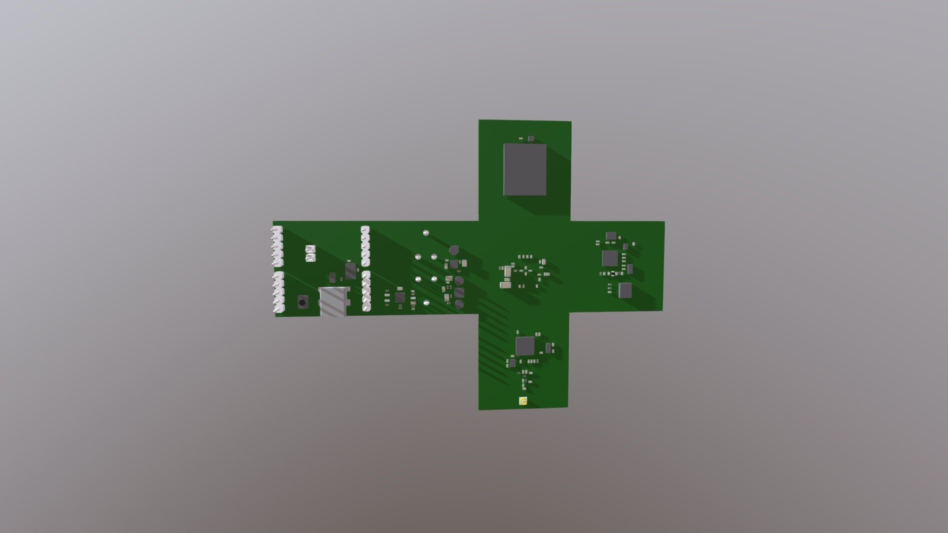
PCB Design Example A Printed Circuit Board (PCB) is a vital component of modern electronics, and its design requires careful planning to ensure efficient functionality. This article will guide you through creating a basic PCB layout using industry-standard tools. Design Requirements The first step in designing a PCB is to define the requirements for the board. This includes determining the type of components that will be used, their quantities, and the space available on the board. The design process starts with creating a schematic diagram of the circuit. Schematic Diagram A schematic diagram is a graphical representation of the electronic circuit. It shows how the different components are connected to each other. To create a schematic diagram, you need to choose a suitable software tool. Popular options include Eagle, KiCad, and Altium Designer. Component Placement Once the schematic diagram is complete, it's time to place the components on the PCB layout. This involves selecting the correct footprint for each component and placing them on the board in the desired locations. Routing The next step is to route the connections between the components. This involves creating a path for the electrical signals to flow through the board. The routing process can be automated using software tools, but manual routing can also be done with practice. Fabrication After the PCB layout has been completed, it's time to send it to the fabrication house. The fabrication process involves cutting out the copper layers and creating the necessary holes for the components. Assembly The final step is to assemble the components onto the PCB. This involves soldering the components onto the board and connecting them to each other using wires or other means. Tips and Tricks Here are some tips and tricks to keep in mind when designing a PCB: * Use a consistent naming convention for your components. * Keep the component placement organized and symmetrical. * Use a grid system to ensure accurate routing. * Avoid overrouting, as it can lead to signal integrity issues. * Use a high-quality solder paste for reliable assembly. Conclusion Designing a PCB layout requires careful planning and attention to detail. By following these steps and tips, you'll be able to create an efficient and functional PCB that meets your design requirements. Remember to always use industry-standard tools and best practices to ensure the highest quality results.
With this file you will be able to print Connected Cube with your 3D printer. Click on the button and save the file on your computer to work, edit or customize your design. You can also find more 3D designs for printers on Connected Cube.